What is a nanostack? Building a chip like a city

Explainer
Peter Hess
To address the rapid escalation in compute requirements for generative AI and foundation models, IBM Research has taken a full-stack approach to building and integrating AI compute into our system products. The IBM Spyre Accelerator emerged from this approach.
Enterprise workloads consist of complex execution flows in which models of various types are used to automate decisions. Integrating AI into enterprise workloads implies that multiple different AI models may be used in various phases of workload execution. This reality requires AI accelerators to have seamless software integration, flexible hardware integration, and enterprise-level robustness and manageability built in. From an AI lifecycle perspective, the need for inference acceleration was the highest initial priority for Spyre. Beyond that, we needed a solution that could be integrated into multiple IBM platforms, especially IBM Z and Power systems. The design choices for Spyre reflect these considerations.
Spyre is the result of a clean-sheet dataflow architecture AI accelerator concept, created in IBM Research. While Spyre is an inference-optimized accelerator, as a key principle we knew it also needed to enable the full lifecycle of AI, namely inference, fine-tuning, and training. We designed the architecture, number formats, and programmability with the generality with that adaptability in mind. This architectural “future-proofing” will enable follow-on versions to cover use cases beyond inference as the needs of our enterprise clients evolve.
Spyre AI cores are designed for mixed-precision AI math. Each Spyre AI core is divided into two “corelets.” A corelet contains a 2D 8x8 SIMD-systolic array for operations like matrix multiplication, and convolution as well as two 1D vector arrays for activation/normalization functions and quantize/dequantize operations. The 2D arrays, each containing 64 low-precision math engines, handle the bulk of the AI computations; the low precision design is fundamental to achieving high energy-performance operation. The 64 engines of the 2D array support low-precision fp16, fp8, int8, and int4 arithmetic. The 1D vector arrays include fp32 capability for operations such as activations that cannot be accurately computed with lower precision operations. Each core’s local memory is a 2-level programmable SRAM scratchpad microarchitecture.
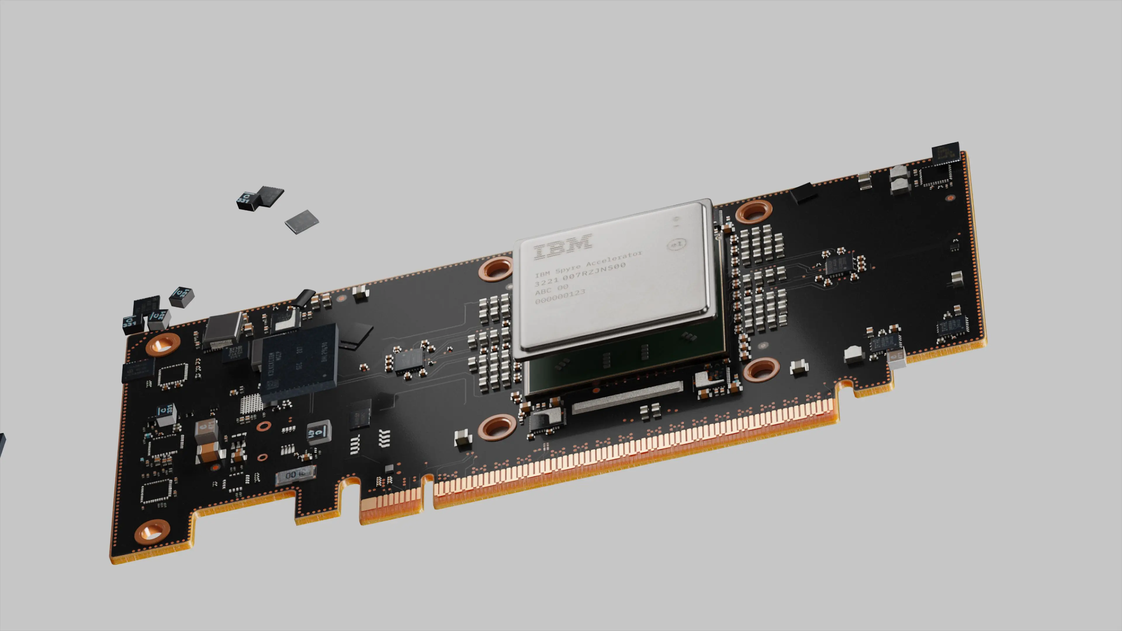
The Spyre system-on-chip (SoC) ASIC contains 32 active cores (plus 2 spares for yield), interconnected via a bi-directional ring. The ring includes an interface to a memory crossbar switch that connects to 16 LPDDR5 channels operating at 6.4 Gbps to deliver 204 GB/sec peak to the cores. LPDDR5 optimizes the capacity-to-bandwidth ratio at low cost per bit while providing sufficient memory bandwidth for the targeted applications. The crossbar has ports for DMA and RDMA engines, which move data over PCIe between Spyre and the host and between multiple Spyres, respectively. The SoC supports fully pipelined DMA/RDMA transfers and execution, allowing these stages to overlap and enabling different phases of independent inferences to run in parallel. The Spyre SoC is implemented in a standard 5nm CMOS technology and contains 25.6 billion transistors.
Spyre is designed to be compliant with the power budget of a single PCIe slot with no auxiliary power connector. To reduce power, we decided to adopt a multiple power domain strategy with a reduced supply voltage of 0.55V for the high activity regions on the chip, and a higher-voltage 0.75V domain for timing-critical and less active regions. Aggressive dynamic power management is important to extract the best performance across various AI models when operating under platform-specific power budgets. Unlike previous solutions to that constraint, Spyre introduces a novel dual-loop power management control mechanism, which enables the peak power to be regulated at two different set-points and two different time constants, controlled by software. This mechanism outperforms single-loop power management schemes.
The Spyre SoC is integrated into a single-slot PCIe card alongside 8 dual-channel LPDDR5 modules and power management control loop circuits. Communicating through a PCIe switch, multiple Spyres form a local group with lowest latency inter-communication, which allows for multi-card operation to aggregate memory bandwidth for performance on generative AI models. Up to 48 of these cards can be deployed in an IBM Z or LinuxONE system, or 16 cards in an IBM Power system to scale AI capabilities.
The Spyre software stack is also essential to the overall accelerator solution. The software partnerships have been developed to ease integration into IBM’s Red Hat Linux-based enterprise software stack. Starting with an inference server and a deep-learning framework, the Spyre software stack, consisting of a compiler, runtime, device driver, and firmware, are invoked to launch inference jobs. Our primary framework is PyTorch 2.x, which is architected to ease accelerator integration. Applications built with PyTorch 2.x can execute on Spyre-powered systems with essentially no software changes.
By employing a unique programmable dataflow microarchitecture and an appropriate spectrum of integer and floating-point number formats, Spyre achieves the inference efficiency, performance levels, and flexibility required for enterprise AI.

